
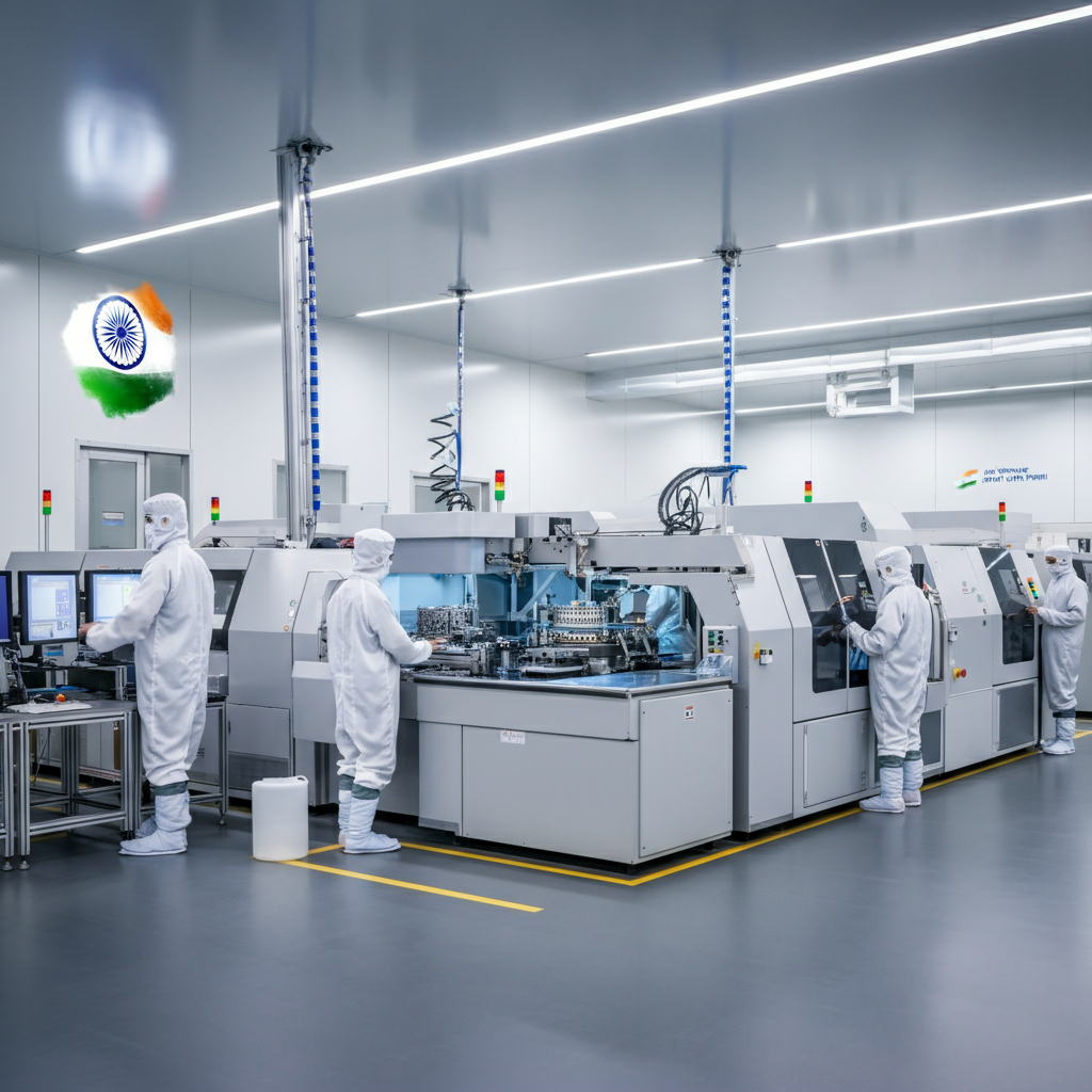
In a major boost to India’s semiconductor industry and mission, The Union Cabinet on Tuesday approved a joint venture worth Rs3,706 crore that is a joint venture between HCL Group and Taiwan’s Foxconn to build the Outsourced Semiconductor Assembly and Test (OSAT) facility in Jewar, Uttar Pradesh. The venture will create over 2000 jobs and help improve the standing of India as a global leader in chip manufacturing.
A Strategic Win for India’s Tech Future
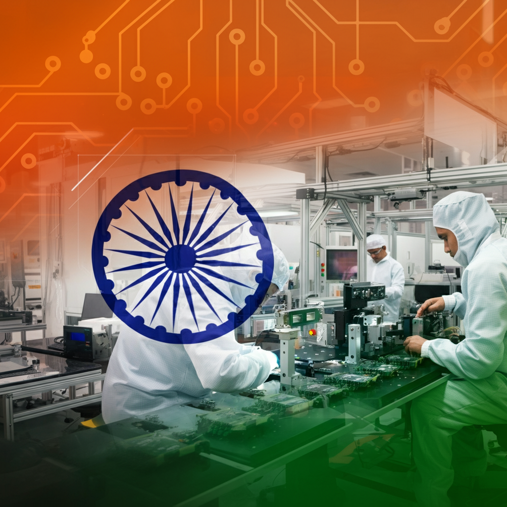
The new facility that is planned for Jewar situated near the under construction Noida International Airport, is a milestone for India’s efforts to decrease dependency on imports of semiconductors. This is the sixth semiconductor plant that has been approved by the India Semiconductor Mission (ISM) and marks Uttar Pradesh’s first OSAT facility.
Get more updates on the latest tech at ArtKerala.com
Key Project Highlights
-
Location: Yamuna Expressway Industrial Development Authority (YEIDA) region, Jewar
-
Investment: Rs3,706 crore
-
Production Capacity: 20,000 wafers/month, ~36 million display driver chips/year
-
Employment: Over 2,000 direct jobs
-
Expected Operations: By 2027
Backed by Government Vision
The project falls within the Center’s strategic roadmap that aims that aims to create India as an world-class semiconductor and electronics manufacturing hub. HCL will be bringing local technology capabilities, as Foxconn will add its top-of-the-line chip manufacturing capabilities.
The government of the UP has been a significant player in offering land and supporting infrastructure and aiming to become an ideal location to future tech investments.
Why It Matters
India is working hard to create a strong semiconductor industry, particularly since the worldwide shortage of chips revealed weaknesses to supply chains. The JV does not just boost India’s ambitions in the field of semiconductors, but also creates a massive opportunities for employment, especially in Tier II regions.
For more comprehensive coverage, go to Economic Times and Reuters.